
 LinkT&B Editorial Department
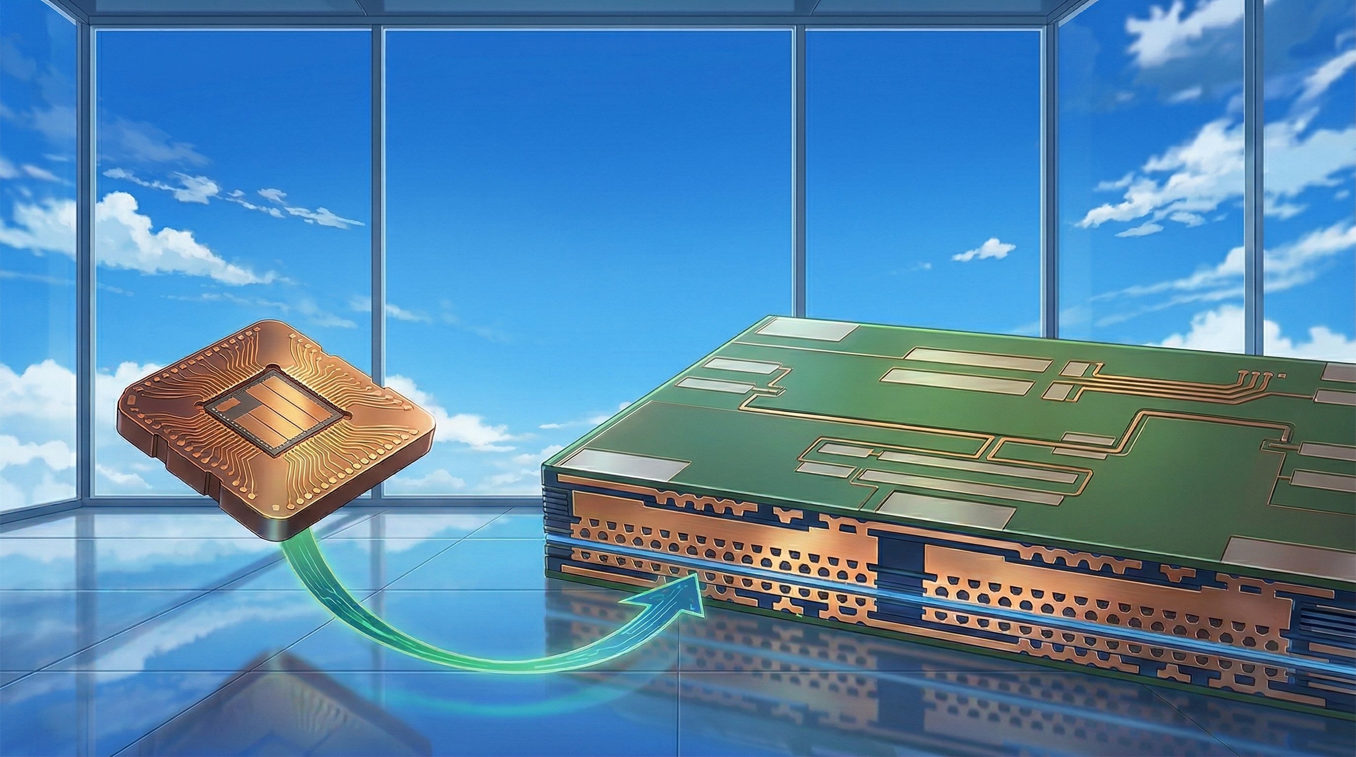
Embedding power semiconductor dies in a PCB brings the die, interconnects and thermal paths into a common package design. Shorter loops can help, but insulation, thermal expansion, connection reliability, inspection and repairability remain central to adoption.
Contents
Checks for an embedded structure
| Item | What to check | How to assess it |
|---|---|---|
| Interconnect | Current loops and joints | Inductance, overshoot and loss |
| Cooling | Path from die to cooling hardware | Junction temperature and thermal resistance |
| Reliability | Expansion mismatch between materials | Thermal cycling and insulation |
| Manufacturing | Tolerances, inspection and yield | Prototype feasibility versus repeatable production |
What changes when components are embedded in a PCB?
Embedding places semiconductor dies or passive components inside a circuit board. It can create shorter current paths than conventional surface mounting. In fast-switching power circuits, the geometry of those paths affects voltage overshoot and ringing. Embedding alone does not solve every thermal or EMC problem: terminals, insulation and cooling must be designed together. Research review on PCB embedding.
Reduce the complete commutation loop
Inductive voltage increases with the rate of change of current. Bring the device and local capacitor close together and reduce the area enclosed by forward and return paths. Long external busbars or connectors can limit the benefit of an improved board.
A universal claim such as “below 1 nH” is not a sound comparison. Use the same measurement terminals, frequency and assembly conditions, then measure gate voltage and power-stage voltage and current. Probe connections can introduce ringing of their own.
Follow the heat path to the cooling surface
Heat passes through conductors, insulation, joints and cooling hardware. Identify the dominant thermal resistances while retaining adequate electrical insulation. Some structures permit double-sided cooling; that is not a property of every embedded board.
Simulation should include interfaces and assembly variation, not just bulk material conductivity. Plan accessible temperature measurements so differences between prediction and prototype can be investigated.
Include insulation, inspection and lifetime testing
Miniaturisation makes electrical spacing, cooling and manufacturing constraints interact. Consider differential expansion, joint fatigue, internal-defect inspection and failure analysis before layout is fixed. Replacing an embedded component is more difficult than replacing a surface-mounted part.
Compare conventional and embedded prototypes under the same voltage, current and cooling conditions. Evaluate waveforms, losses and temperature together with manufacturing cost, inspection and yield. LinkT&B supports power-electronics circuit design and experimental evaluation.
Discuss your project
We support circuit design, prototyping and hardware testing. Tell us about the operating conditions and the problem you need to investigate.