
 LinkT&B Editorial Department

Investigate FET switching noise through parasitic inductance, capacitance, gate drive and measurement setup. Slower switching can increase losses, so compare waveforms, temperature and efficiency under the same conditions.
Contents
- Measurements to retain before and after a change
- The true nature of noise: 4 mechanisms of generation
- First layer of countermeasures: board layout
- Second layer of countermeasures: Gate drive optimization
- Third layer of countermeasures: Snubber circuit
- Fourth layer of protection: shields and filters
- What will and will not change in the SiC/GaN era
- Summary: Checklist for the 4-tier approach
- Please contact us
- Reference materials
- Related Articles
- Discuss your project
Have you ever been designing a power electronics circuit and faced problems such as “If I raised the board, it failed an EMI test” or “the control microcontroller malfunctioned”? Many of these problems are caused by noise caused by the switching operation of power MOSFETs and IGBTs. In particular, next-generation power devices such as SiC and GaN have switching speeds that are orders of magnitude faster than conventional Si-MOSFETs, and the noise frequency band also shifts to the higher frequency side, so there are an increasing number of cases where traditional design methods no longer apply.
In this article, we classify the generation mechanisms of FET switching noise into four types and explain practical countermeasures for each using the four-layer structure of “board layout,” “gate drive,” “snubber circuit,” and “shield filter.”
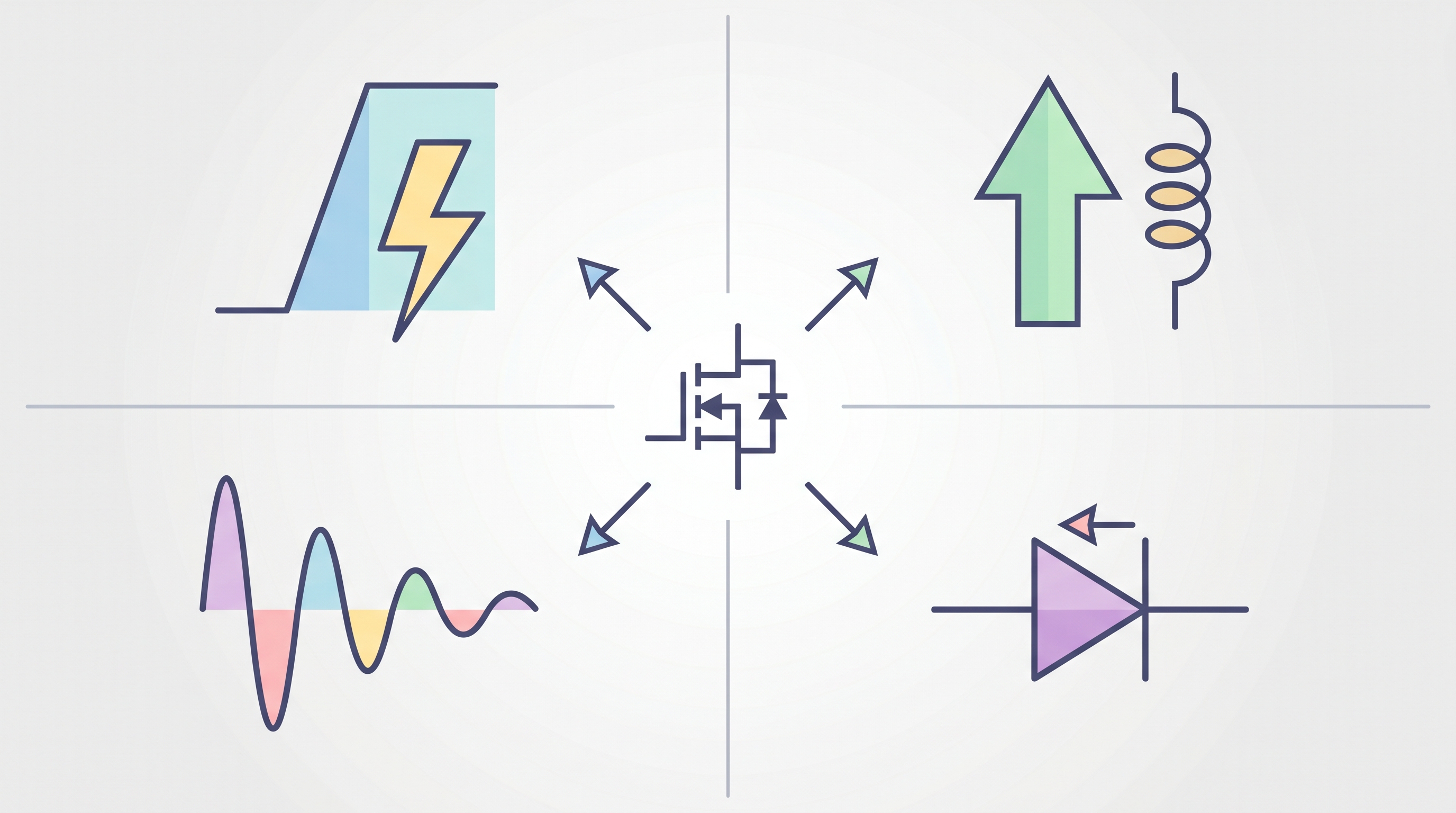
Figure 1. Four main generation mechanisms of FET switching noise. From the center FET in all directions, upper left: steep voltage change (dV/dt), upper right: interaction between current change and inductance (dI/dt), lower left: ringing oscillation due to parasitic LC, lower right: reverse recovery current (recovery) of the body diode. These four elements interact to produce noise.
Measurements to retain before and after a change
| Item | What to check | How to assess it |
|---|---|---|
| Waveforms | VDS, VGS and current | Overshoot, ringing and false turn-on |
| Measurement | Probe, connection and bandwidth | Identify probe-induced ringing |
| Trade-offs | Losses, temperature and efficiency | Evaluate more than noise reduction |
The true nature of noise: 4 mechanisms of generation
1. dV/dt noise (displacement current noise)
When a MOSFET turns on and off, the drain-source voltage changes rapidly. The larger this voltage change rate (dV/dt) is, the more displacement current flows through the FET's drain-gate capacitance (Cgd, Miller capacitance) and the device's parasitic capacitance, which propagates to surrounding signal lines and control systems as noise. In SiC-MOSFETs, dV/dt reaching several tens of V/ns is not uncommon, and under typical conditions it tends to be larger than that of conventional Si devices (there are differences depending on whether the comparison target is Si-MOSFET or IGBT, voltage class, gate resistance, and package).
2. dI/dt noise (inductive noise)
This is the voltage spike that occurs as the product of the rate of change of current during switching (dI/dt) and the inductance of the wiring and package (parasitic inductance Ls), that is, V = Ls × dI/dt. In board layouts with long main current loop traces or high inductance, this spike can cause ground bounce and gate signal disturbances. GaN devices have current rise times on the order of nanoseconds, so a parasitic inductance of just 1 nH can result in a spike of several volts.
3. Ringing
The damped oscillation (ringing) seen immediately after switching is caused by the LC resonant circuit formed by the inductance and capacitance in the circuit. The frequency of this ringing can reach tens of MHz to hundreds of MHz and is a major source of radiated noise. Voltage ringing at the switching node can lead to serious EMI problems, especially in circuits where the upper and lower arms alternately switch in a half-bridge configuration.
4. Diode recovery current
When the body diode or external freewheeling diode switches in the opposite direction, accumulated carriers are swept out, causing a reverse recovery current to flow. This current has large instantaneous peaks and generates spikes along the same path as dI/dt noise. Si-PIN diodes have relatively long reverse recovery times and large reverse recovery currents, so replacing them with SiC-SBDs (Schottky barrier diodes) is effective in reducing noise.
First layer of countermeasures: board layout
The foundation of noise countermeasures is board design. It is much more effective to minimize parasitic inductance during the layout stage than by adding components later.
The most important thing is to minimize the area of the main current loop. By keeping the loop from the DC input capacitor to the FET to the return path as short and small as possible, you can reduce both loop inductance and radiation. Specifically, the basic design is to place the input bus capacitor in close proximity to the FET, and to place the power plane and return plane on adjacent layers to allow current to flow through the plane.
Keep the gate drive loop small as well. If the loop connecting the gate driver IC, gate resistor, and FET gate-source terminal is large, it will be easier to pick up inductive noise from the main current loop. Ideally, the distance between the gate driver and FET should be as close as possible, and the source return should be separate from the main current return path.
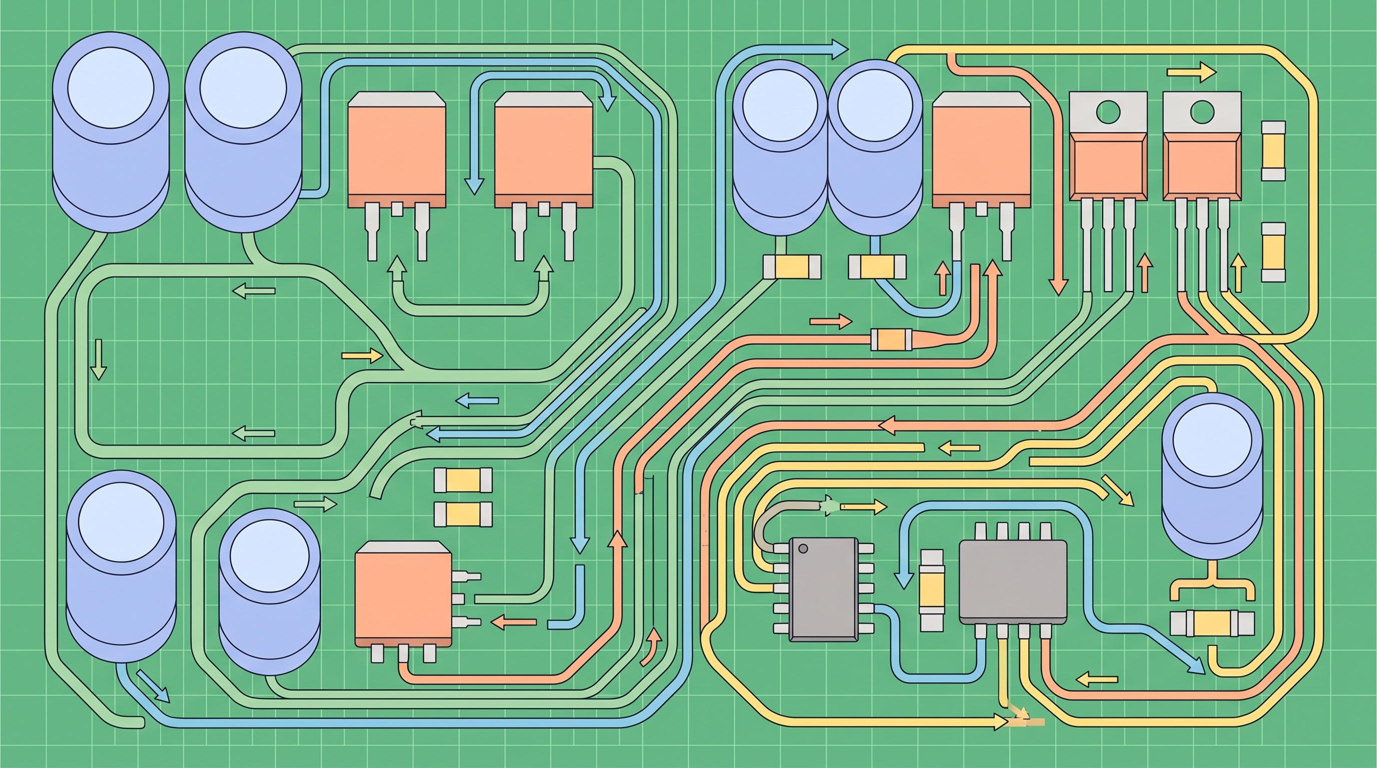
Figure 2. Board layout essentials: minimizing main current loop area and separating gate loops. Reducing parasitic inductance is the foundation of noise countermeasures.
Second layer of countermeasures: Gate drive optimization
Controlling switching speed is a trade-off between noise and switching losses. Increasing the gate resistance (Rg) will make dV/dt and dI/dt more gradual and reduce noise, but switching loss will increase. Conversely, reducing Rg will reduce loss due to high-speed switching, but will increase noise.
In practice, it is common to separate the turn-on resistance (R_on) and turn-off resistance (R_off) and adjust them independently. Specifically, a diode is used between the gate driver output and the gate terminal to separate the charging and discharging paths, and different resistance values are set for each. You can set the optimal drive speed for each transition, controlling dI/dt at turn-on to suppress recovery noise, and controlling dV/dt at turn-off to suppress ringing.
Among the latest gate driver ICs for SiC and GaN, products with programmable control of slew rate have also appeared. For example, Texas Instruments' UCC217xx series can independently adjust turn-on/turn-off using a split output or external gate resistor, and Infineon's EiceDRIVER 2L-SRC/SRC Enhanced family has built-in slew rate control. Utilizing these products will lead to a reduction in evaluation man-hours.
Third layer of countermeasures: Snubber circuit
If ringing cannot be completely suppressed by optimizing the board layout and gate drive, residual vibrations can be absorbed by a snubber circuit.
| Snubber type | configuration | Features | Applicable scene |
|---|---|---|---|
| RC snubber | Resistor + capacitor series | Easy to design, effective over a wide range of frequencies | General purpose ringing suppression |
| RCD snubber | Resistor + capacitor + diode | Selectively clamp turn-off spikes | Flyback, forward converter |
| active clamp | Regeneration with FET + capacitor | Energy regeneration possible, low loss | High power applications requiring high efficiency |
As a simple guideline for selecting RC snubber constants, first measure the ringing frequency f_ring with an oscilloscope, then roughly estimate the snubber capacity from Cs ≈ 1/(2π × f_ring × Rs). The starting point for the snubber resistance Rs is basically around the ringing impedance √(L/C). However, this formula is only for estimating the initial value, and in reality, the practical approach is to repeatedly check the waveform and make fine adjustments on the actual device, taking into account the inductance of the snubber arrangement, withstand voltage margin, power dissipation, etc.
Fourth layer of protection: shields and filters
The measures taken so far are approaches to suppressing the “source” of noise, but as a final step, measures to prevent radiated and conducted noise from “escaping” are also necessary.
As a countermeasure against conduction noise, place an EMI filter that combines a common mode choke coil and an X capacitor and a Y capacitor on the power input line. When designing a filter, use a spectrum analyzer to identify the peak frequency of the noise, and select constants that provide sufficient attenuation in that band.
As a countermeasure against radiation noise, it is effective to surround the power stage with a metal casing or shield plate. However, the effectiveness of the shield greatly depends on the quality of the ground connection, so the connection between the shield plate and the board GND must be made reliably with low impedance.
What will and will not change in the SiC/GaN era
Even if SiC and GaN devices become widespread, the physical mechanism of noise generation itself will not change. What changes are the frequency band and the magnitude of the effect.
As a typical example, Si devices have a switching frequency of several tens of kHz to several hundred kHz and a ringing frequency of several MHz to several tens of MHz, whereas in SiC/GaN, the main switching frequency increases to several hundred kHz to several MHz, and ringing can reach tens of MHz to several hundred MHz (the exact values vary depending on the voltage class, current, gate drive conditions, and package). In this band, even short wiring on the board can easily function as an antenna, causing the problem of radiated noise.
Therefore, layout becomes even more important in SiC/GaN designs, and short traces and small loops, which were previously a "best practice", become a "must have". An approach that visualizes parasitic components at the design stage using simulation tools (EMC analysis from Ansys and Keysight) directly leads to a reduction in the number of prototypes.
Summary: Checklist for the 4-tier approach
- Layer 1 board layout: Minimize main current loop area, separate gate loops, utilize power planes
- 2nd layer gate drive: Separate adjustment of turn-on/turn-off resistance, consideration of slew rate control IC
- Third layer snubber circuit: Measures ringing frequency and absorbs residual vibration with RC snubber or RCD snubber
- 4th layer shield filter: Conducted noise suppression with EMI filter, radiated noise suppression with shield
Noise countermeasures cannot be solved with "one silver bullet," but the basic strategy is to deal with them in layers at each phase of the design. Especially in the SiC/GaN era, noise, surge, and efficiency are greatly influenced by layout, so optimization at the board design stage will make the difference between success and failure.
Please contact us
LinkT&B provides a wide range of services, from EMC design support for power electronics circuits to commissioned development of power conversion circuits using SiC/GaN. If you have any issues such as "I can't pass the EMI test" or "I want to replace the existing circuit with SiC", please visit the R&D/Power Electronics Business page or contact us directly from Contact Us.
Reference materials
- Texas Instruments, "Fundamentals of MOSFET and IGBT Gate Driver Circuits" (Application Note SLUA618)
- Infineon Technologies, "Gate Driver ICs for SiC MOSFETs — Application Note"
- ROHM Semiconductor, "Basic knowledge of SiC power devices"
- Nexperia, "GaN FET Application Guide"
Related Articles
Choosing a Power Electronics Development Partner in the SiC/GaN Era / Five Pitfalls to Avoid When Deploying Generative AI at Work
Further reading: Infineon: gate-drive and layout recommendations
Discuss your project
We support circuit design, prototyping and hardware testing. Tell us about the operating conditions and the problem you need to investigate.